Proposal of Spin Generation Scheme in Semiconductor with the Highest Efficiency
Research Press Release | November 06, 2015
-
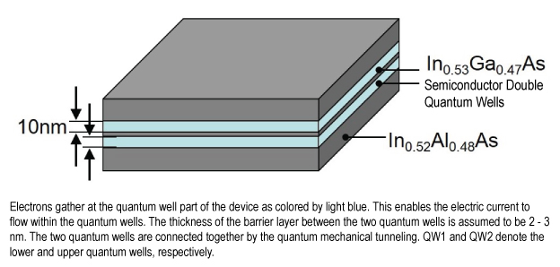 Fig. 1 Semiconductor double quantum well schematic
 -
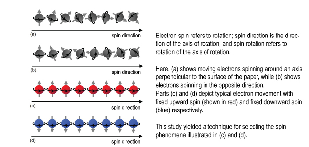 Fig.2 Spin direction
| Press Release | ||
|---|---|---|
| Key Points |
・This study demonstrated that semiconductor double quantum wells processed properly at the sub-micron scale can be used to boost the current-induced spin1 density to more than 10,000 times relative to the previously observed values. This marks a new step toward the next-generation electronic device development based on the spin degree of freedom. ・The scheme of semiconductor band engineering2 was used to illustrate the detailed mechanism how the complete spin blocking can take place by applying a magnetic field parallel to the plane of the quantum well. ・The fact that the spin-orbit interaction3 in the semiconductor double quantum well connects the two wave functions with different parities4, the so-called interband Rashba effect, played an essential role in this discovery. |
|
| Overview | In a joint study with Kobe University, Keio University, and NTT, a research team led by Associate Professor Takaaki Koga at the Graduate School of Information Science and Technology, Hokkaido University has proposed a new approach for screening conduction electrons depending on their spin states. The new approach utilizes the spin-orbit interaction in a semiconductor double quantum well composed of indium, gallium, aluminum and arsenic (see Figure 1). Specifically demonstrated in this research by applying an external magnetic field parallel to the quantum well surface is the vivid mechanism of the spin selection for the conduction electrons. The research team was able to demonstrate the spin selection mechanism of 100% efficiency illustratively by analyzing the anticipated orbits of electrons in real space for each spin separately.
Spin-orbit interaction is understood as the measure of the easiness for electron spins to be controlled by the transistor gate. The precise value to characterize it for the semiconductor system used in this study, what is called the intrinsic constant for the Rashba effect, had not been determined precisely until even a few years ago.5 The research team paid attention to the fact that the spin-orbit interaction in a semiconductor double quantum well can connect two wave functions with different parities, as is called the interband Rashba effect. The conclusion they reached is that the generation of spin by electric current, termed as the “current induced spin polarization” or “Edelstein effect”, 6 should be boosted by a factor of more than 10,000 relative to the existing experimental values with the conventional semiconductors by processing properly the carefully designed semiconductor double quantum well at a sub-micron scale. Use of the spin degree of freedom in semiconductor devices is regarded as providing a key to the development of next-generation electronic devices such as field-effect spin transistors, quantum computers, and ultra-low-power-consumption devices. This study has demonstrated a way to significantly boost the Edelstein effect, which, together with the spin-Hall effect7 constitutes the two major spin generation schemes in nonmagnetic semiconductors. Consequently, it illuminates a promising new direction for the development of future electronic devices based on the spin degree of freedom and gives a major impact on device research and development in the industry. This study was conducted with funding from Grant-in-Aid for Scientific Research (B), KAKENHI, No. 23360001. |
|
| Terms |
1 Spin states Electron spin refers to rotation; spin direction is the direction of the axis of rotation; and spin rotation refers to rotation of the axis of rotation (See Fig.2) 2 Semiconductor band engineering A technique for designing and developing semiconductor materials and devices with specific properties and functionality in which physical properties can be predicted via relatively simple theoretical quantum mechanics calculations using nanoscale materials for bonding non-identical semiconductors. This technique was proposed by Nobel physics prize winner, Leo Esaki. 3 Spin-orbit interaction The relativistic effect whereby electrons moving at high speed through an electrostatic field interpret an electric field as the influence of a magnetic field, even in the absence of an actual magnetic field, so that the force is received by the magnetic moment of the spin. For a narrow gap semiconductor such as InGaAs in this study, the relativistic effect can be up to 1,000,000 times stronger than the effect in a vacuum. 4 Parity In simple terms, parity indicates whether the wave function is odd or even. 5 Related research Determine the scale accuracy of spin-orbit interaction level. Hokkaido University and NTT, Accelerated Development of Next-Generation Elements, Nikkan Kogyo Shinbun, 2011.3.15 6 Edelstein effect Electric current passing through the electron system (two-dimensional electron gas) formed at the surface of the sample material or the interface of differing materials causes the entire sample to be magnetized, even when the sample material is nonmagnetic. Actual observation of the Edelstein effect was by Kato et al. in 2004. 7 Spin-Hall effect Electric current passing through a nonmagnetic metal substance or semiconductor generates an electron spin flow (magnetism flow) perpendicular to the current direction. The spin-Hall effect has important implications for spintronics, where current is replaced by spin flow. |
|
| Important points |
(1) This study demonstrated that semiconductor double quantum wells processed properly at sub-micron scale can be used for enhancing the current-induced spin polarization by more than 10,000 times relative to the previously reported experimental values. Such accomplishment should mark an additional step forward in the electronic device development of next generation based on the spin degree of freedom of electron. (2) The exact mechanism how the proposed spin blocking takes place was illustrated in a magnetic field applied parallel to the planes of the quantum wells using the scheme of semiconductor band theory. (3) An important discovery in 2007, that the spin-orbit interaction in the semiconductor double quantum well connects the two wave functions with different parities, which is called as the interband Rashba effect [Bernardes2007], plays an essential role in the present device prediction. Through joint research with Kobe University, Keio University, and NTT, my students and I proposed a new approach for screening conduction electrons depending on their spin state. This new approach utilizes a semiconductor double quantum well that is composed of indium, gallium, aluminum and arsenic. Demonstrated in this work was the vivid mechanism of electron selection by its spin state, for the conduction electrons, with an external magnetic field applied parallel to the quantum well planes. We were able to show a 100% efficiency of spin selection, illustratively, by analyzing the calculated motions of electrons in real space for each spin state separately. Spin-orbit interaction (or the Rashba Effect) is understood as a measure of the ease for electron spins to be controlled by the gate voltage of transistor. The precise value to characterize it, which is called as the intrinsic constant for the Rashba effect, had not been clarified for any semiconductor materials even until a few years ago. We paid attention to the fact that the spin-orbit interaction in a semiconductor double quantum well can connect two wave functions with different parities (interband Rashba effect). The conclusion we reached was that the generation of spin by electric current, termed as the Edelstein effect, should be enhanced at least by a factor of 10,000 relative to the experimental values reported with conventional semiconductors, by processing properly at sub-micron scale the semiconductor double quantum wells that are carefully designed for this purpose. The present work shares the common basic idea with the paper I published previously: Spin-filter device based on the Rashba effect using a non-magnetic resonant tunneling diode, T. Koga, J. Nitta, H. Takayanagi and S. Datta, Physical Review Letters 88, 126601 (2002) [Koga2002a], which has been cited more than 350 times by now. The main idea I presented there was obtained during discussion with Dr. J. Nitta at NTT Basic Research Laboratories. The idea was then refined following discussion with Professor S. Datta at Purdue University in March of 2001, when Dr. Nitta and I visited him under a project of NEDO (New Energy and Industrial Technology Development Organization, Project No.00MB3) that Dr. Nitta was leading then. The experimental realization of this 2002 idea turned out to be difficult. The main obstacle was p-doing at the barrier layer between the two quantum wells that constitute the RTD (Resonant Tunneling Diode). We needed this p-doping to enhance the interband Rashba effect in the RTD device in the present terminology. It took some years until I came up with the idea of using lateral transport of electrons in double quantum wells for realizing basically the same physics as in the 2002 paper. The concept of the interband Rashba effect in a symmetric double quantum well (QW) had been well-established by that time. By carefully examining the material parameters of the system we had been using in our experiments, we concluded that spin selection is possible by tuning the device length, gate electric field and in-plane magnetic field utilizing the interband Rashba effect as in the present work. We particularly showed illustrative mechanisms using a one-dimensional model with a wave vector k=(kF, 0), where the selected spin can be blocked completely in the presence of the in-plane magnetic field. While the inclusion of the finite ky and/or the gate electric field deteriorates the spin polarization P, finite values remains for P (P>11% ) even without the magnetic field. |
|
| Inquiries |
Takaaki KOGA, Assoc. Professor, Division of Electronics for Informatics, Graduate School of Information Science and Technology, Hokkaido University TEL: +81-11-706-6539 FAX: +81-11-706-7803 E-mail: koga[at]ist.hokudai.ac.jp |
|
|
Japanese Link |
半導体における最大効率のスピン生成法を提案 (2015.9.30) | |
| Publications | Spin blocker using the interband Rashba effect in symmetric double quantum wells, Physical Review Applied (2015.9.29) | |